Polishing Pads

Advanced CMP Polishing Pads for Semiconductor Planarization

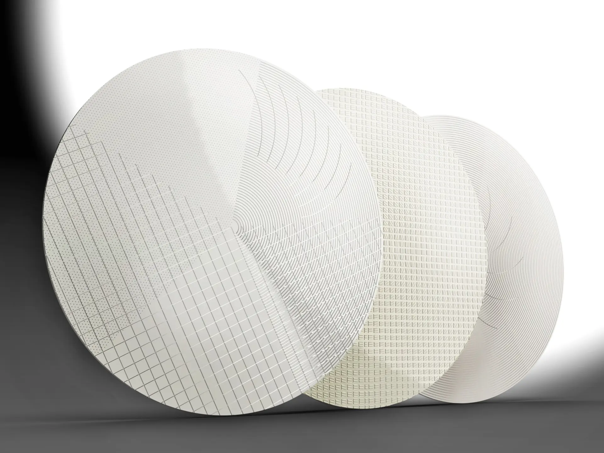
We deliver CMP polishing pads engineered for reliability, consistency, and high-quality wafer results. Designed with advanced patterns and membrane structures, our pads support the most demanding semiconductor planarization processes.

Whether you are polishing copper, tungsten, oxide, or dielectric layers

Our pads ensure:
Superior planarity and surface integrity
Efficient slurry distribution for predictable results
Reduced defects and improved wafer yield
Longer pad life and optimized cost-of-ownership

With multiple textures and groove patterns available, our CMP pads offer a perfect balance between precision, stability, and durability—empowering fabs to achieve cleaner surfaces and better device performance.